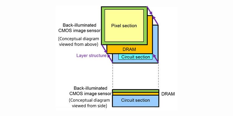
Sony on Tuesday announced its first 3-layer stacked CMOS image sensor with DRAM for smartphones. The company is promoting that the new CMOS sensor for smartphones will be the first in the industry to include a DRAM layer.
Sony adds that apart from the DRAM layer added to the conventional 2-layer stacked CMOS image sensor, a layer of back-illuminated structure pixels and a chip affixed with mounted circuits for signal processing are also present. With the new CMOS image sensor, Sony claims smartphones can support 1080p (1920×1080 pixels) resolution video at up to 1,000 frames per second (fps). The Japanese company believes that the DRAM layer enables the sensor to deliver fast data readout speeds which will make it possible to capture still images of fast-moving subjects with minimal focal plane distortion as well as super slow motion videos.
“In order to realize the high-speed readout, the circuit used to convert the analogue video signal from pixels to a digital signal has been doubled from a 2-tier construction to a 4-tier construction in order to improve processing ability. Although there are speed limitations in the interface specifications for outputting signals from image sensors to other LSIs, this sensor uses DRAM to store signals read at high speed temporarily, enabling data to be output at an optimal speed for the standard specifications. As a result, the product is capable of reading one still image of 19.3 million pixels in only 1/120 of a second (approximately 4x faster than conventional products*3), thereby supporting high-speed image capture,” explains Sony in a press statement.
Sony announced the development results of the all-new CMOS image sensor at the recent International Solid-State Circuits Conference (ISSCC) in San Francisco. The new Sony CMOS image sensor is claimed to be eight times faster than the Sony IMX318.
[“source-ndtv”]
